Compact Modeling
Two-Resistor Compact Models
Theoretical Basis
Introduction
Creating validated compact models of electronic packages has always been a challenge in the electronics industry. Traditional metrics such as junction-to-case thermal resistance and junction-to-ambient thermal resistance are sometimes useful as figures of merit, but can give errors as large as 100% or more in real environments.
An improvement in the accuracy of the metrics can be obtained by extending the concept to two resistors, or links. Such a model is the simplest possible network compact model, and is defined as being constructed out of two resistance values - a junction-to-case resistance (Rjc) and a junction-to-board (Rjb) resistance. Note that both these values are to be obtained from tests.
Figure 6-1.
A 2-Resistor Network Compact Model

Two-resistor models have the following advantages:
- Their structure is intuitive
- They are test-based
- They are likely to give acceptable accuracy for design parametrics
- They represent a large increase in accuracy for prediction of absolute results as compared to the traditional single-resistor metrics
JEDEC Tests
One of the biggest advantages of Two-Resistor models is that they are based on standard JEDEC tests rather than analysis.
The junction-to-case resistance (Rjc) is normally derived from a “Top Cold Plate Test”, in which the package is placed on a board with all sides insulated except the top surface. A cold plate at a specified temperature is pressed against the top surface, hence, most of the power dissipated from the package leaves through its top (isothermal) surface. The one-dimensional equivalent of Fourier’s law is then applied to derive Rjc. Thus,
Rjc = (Tj - Tcld)/P
Where Tj is the junction temperature and Tcld is the temperature of the cold plate.
The junction-to-board resistance (Rjb) is derived by placing the package in a specially constructed harness known as the Ring Cold Plate. (This method has now been formalized as a JEDEC standard, ref 1.) The Ring Cold Plate (Figure 6-2) fixture consists of a standard 4-layer JEDEC board (ref 2) inserted between two cold plates. The cold plates are in the shape of a “ring”. Thus heat travels from the package through some distance within the board, and then out of the fixture through the coolant fluid in the cold plate.
Figure 6-2.
Package in a Ring Cold Plate (FloTHERM Model)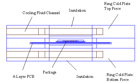
Rjb is calculated by using the one-dimensional version of Fourier’s law:
Rjb = (Tj - Tb)/P
The board temperature (Tb) is taken as the temperature at a point on the board surface located in the middle of the longest side of the package, no more than 1 mm from the package edge.
The FloTHERM PACK Approach
The approach taken in FloTHERM PACK is to essentially “shadow” the experimental methodology (Figure 6-3). Thus the detailed model is placed in the respective harnesses. The two simulations are then run on the FloTHERM PACK server using a conduction solver to solve for the temperatures and fluxes. The resistor values are then computed from the solution temperature fields. (All of this is transparent to the user.)
On completion of a run, a notification email is sent to the email address specified in Preferences > Account Information.
In order to comply with the JEDEC specification, two versions of the Ring Cold Plate are used: one for packages less than 30 mm size, and the other for packages larger than 30 mm.
The manner in which the Top Cold Plate test is implemented is an idealized version of what an actual experiment might look like. Thus, instead of actually solving for a package on a test board with a top cold plate, FloTHERM PACK applies an isothermal boundary condition on the package top surface, and adiabatic boundary conditions on all other surfaces. This creates an idealized version of the Top Cold Plate Test.
Figure 6-3.
Generating Two-Resistor Compact Models in FloTHERM PACK

Generating a Two-Resistor Compact Model
The FloTHERM PACK implementation follows the methodology outlined above. The following additional points should be noted:
- The detailed model used for generating the compact model is the one that would be consistent with the CFD modeling choices selected by the user. In other words, changing these choices in the design sheet changes the compact model, such that the network is always derived from the selected detailed model.
- The compact model downloaded is in the FloTHERM PDML file format.
- Once the compact model is imported in FloTHERM, it will be seen as a "Compact Component SmartPart". The variables within the SmartPart will not need to be changed, and the user is advised to leave the menus alone. The only exception to this is the heat (power) dissipation, which can be changed if the user wishes to run the compact model for a different power mode. (Note that a Two-Resistor compact model is independent of power for a single-die package.)
Let us take a walk-through of the steps you would take in order to generate a Two-Resistor compact model.
Submitting a Two-Resistor Compact Model Job
In the library menu for your part in FloTHERM PACK, click on the Compact Model tab. This screen displays any compact models associated with the library item, and provides options for creating a new compact model, see Figure 6-4.
Figure 6-4.
Creating a New Two-Resistor Model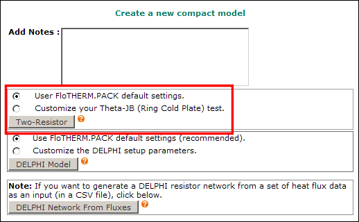
- You can add notes to your compact job if you wish. These notes are saved with the compact model job you create.
- The Two-Resistor button has two radio buttons associated with it. The recommended option is User FloTHERM PACK default settings which uses defaults and submits the compact model job without requiring any further details.
However, if you wish to customize your two-resistor model generation environments (specifically, the Theta-JB test), then choose Customize your Theta-JB (Ring Cold Plate) test. You will then be taken to the test PCB wizard menu where you will be able to choose a different PCB and customize the % metal coverage of each copper layer (except for the Top Layer coverage of packages identified in "Detailed Trace Modeling"). You will also be able to add vias to the test PCB.
Click the Two-Resistor button to submit the job. You will get a message confirming your submission, similar to the example shown in Figure 6-5.
Figure 6-5.
Two-Resistor Compact Model Submitted
Once a job has been submitted you can monitor its progress as described in “Monitoring the Job Status”.
Examining the Results
You can access the results of your model by clicking on the icon for the job in the Compact Model tab of your library. The two resistors comprising the compact model, Theta-JC and Theta-JB, will be listed, see Figure 6-6.
Figure 6-6.
Two-Resistor Compact Model Results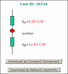
Notes
- In Version 3.3 all compact models were placed in the default Compact folder. In V4, the Compact folder is no longer used and all compact models are fully integrated with the library to which they belong. Legacy compact models for each user have been assigned to their libraries of origin whenever possible. Those legacy compact models for which original libraries could not be located will still be available in the Compact folder as individual library items, but can be moved or deleted by users.
- After a compact model has been generated, you can change the values in the design sheet. If you do this, the compact model archived in the library will no longer correspond to the part reflected in the design sheet data. If you think you have changed your design sheet data subsequent to the generation of the compact model, click on the Case ID link to recover your design sheet.
- A tick
 under the Notes column indicates the most recently-generated compact model for the particular library.
Downloading a Two-Resistor Compact Model
You have two options for downloading a compact model as a PDML file, see Figure 6-6. In both cases you can choose to either open the PDML file, which will open FloTHERM if installed, or save the file to a folder.
- Download as Compact Component downloads the compact model as a FloTHERM Compact Component.
- Download as Network Assembly downloads the compact model as a FloTHERM Network Assembly.
Two-Resistor Compact Models in FloTHERM
When you open a downloaded compact model in FloTHERM it will appear as either a Compact Component SmartPart (Figure 6-7) or as a Network Assembly (Figure 6-8), depending on which option was chosen when downloading the PDML file.
Figure 6-7.
Compact Model as a FloTHERM Compact Component
Figure 6-8.
Compact Model as a FloTHERM Network Assembly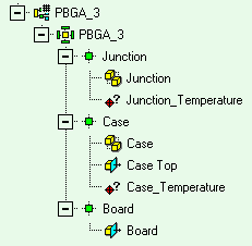
The Compact Component SmartPart object is simply a FloTHERM implementation of a thermal resistance network. For more information, please consult the FloTHERM on-line help.
Heatsink Clearances
For packages for which the contact area with a heatsink is significantly smaller than the substrate area (for example, flip-chip or capped packages), the two-resistor Compact Component SmartPart comes with a concentric “ring” of collapsed cuboids (in the assembly called heatsink clearance) that essentially mimics the clearance between the region outside the die and the heatsink. Thus the collapsed cuboids are assigned a thickness equal to the clearance and a conductivity of air. This ensures that the area of heat transfer to the heatsink is correctly sized when a heatsink model is placed on top of the compact model. By default, these collapsed cuboids are de-activated, see Figure 6-9, and if your application does not involve adding a heatsink to the package, it is advisable to leave them de-activated.
Figure 6-9.
De-activated Heatsink Clearances in Compact Component SmartPart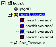
References
- JEDEC Standard, High Effective Thermal Conductivity Test Board for Leaded Surface Mount Packages, JESD 51-7, https://www.jedec.org
- Sarang Shidore, Gary Kromann & Steve Addison, Development of Optimized Component-Level Thermal Behavioral Models of a Plastic-Ball-Grid Array Interconnect Technology For Air Cooled Applications, Proceedings of InterPACK ’97 Conference, June 1997, Hawai’i, U.S.A.
- Bennett Joiner and Vance Adams, Measurement and Simulation of Junction-to-Board Thermal Resistance and its Application in Thermal Modeling, Proceedings of SEMITHERM XV, March 1999.