Micro-BGA
Introduction
Micro Ball Grid Array (Micro-BGA™) characteristics:
- Chip-scale package from Tessera Inc. (that is, package size no greater than 20% of the die size)
- Solder balls for 2nd level interconnect
Applications of Micro-BGAs:
- Flash memory
- Consumer electronics (for example, cell phones)
General Thermal Considerations
Micro-BGAs, being Chip Scale Packages (CSPs), are inherently limited in the amount of heat they can dissipate.
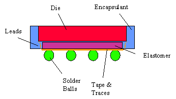
Figure 5-13.
Structure of a Micro-BGA
Micro-BGAs tend to have most of their heat flow through the solder balls to the board. This is due to the small die area available for heat transfer to the air, and the difficulty of adding a heatsink.
Modeling Options
The Die and is modeled using a cuboid.
Due to the low conductivity of the elastomer material, the substrate usually offers a relatively high thermal resistance. So does the Encapsulant.
The leads connecting the die edges to the trace layers present on the tape tend to transfer a relatively small amounts of heat, especially for the smaller Micro-BGAs. Hence, they are not included in the model. However, you should check this assumption for the larger packages.
The solder balls connecting the package substrate to the board are modeled discretely. This is because the spreading or "flux?crowding" resistance as the heat flows from the package to the board can be a significant portion of the overall package resistances, especially for smaller packages. Hence you are not given options to lump the solder balls in any way.
Material Properties
Thermal conductivities:
Typical encapsulant and elastomer material: 0.4 - 0.6 W/(m.K)
Polyimide: 0.2 W/(m.K)
37Pb/63Sn solder: 50 W/(m.K)
Copper: 390 W/(m.K)